
Electrode formation technologies for power device products, semiconductor lasers, and optical communication device substrates.
- Jun 18, 2022
- 5 min read
Updated: Jul 20, 2024

Hello! I'm TZ of sales department.
The power semiconductor market is currently expanding in response to energy conservation due to tight global electricity demand and the need to take measures against global warming.
In the automotive industry, the demand for power modules, primarily silicon IGBTs, is growing with the spread of hybrid and electric vehicles (HV/EV). To meet the growing demand for power semiconductors, mass production plants of overseas power semiconductor manufacturers are increasing production capacity by shifting wafer sizes to 12 inches. Following the trend of overseas manufacturers, domestic power semiconductor manufacturers have also announced large-scale capital investment plans, including 12 inches mass production lines.
In some packaging processes for next-generation power semiconductors, electrode formation such as for semiconductor lasers and optical communication devices, electrodes and wiring are formed by electroplating after patterning using photolithography.
A common technical challenge is how to deal with localized heat generation in the chip area. As products become more compact and larger in current and frequency, localized heat generation occurs internal stress due to mismatches in coefficient of thermal expansion (CTE) of materials such as chips, boards, wiring, and resins, which can cause substrates warpage and chip and wiring breakage, significantly affecting product yield and reliability.
In this article, we’d like to introduce the activities that Tosetz is engaged in to develop the electrode formation technology required for the electronic devices mentioned above.
Next-generation power semiconductors, wide band gap (WBG) semiconductors
Next-generation power semiconductors, such as silicon carbide (SiC), gallium nitride (GaN), and gallium oxide (Ga2O3), are seen as promising candidates for applications such as in-vehicle inverters and 5G wireless communications, whose markets are expected to expand further in the future.
The electrodes of power semiconductors are generally formed using UBM (Under Barrier Metal), which is an electroless NiAu or NiPdAu plating film formed on the underlying aluminum pad, or gold bump plating formed by electroplating.
However, we are now in an era where power semiconductors are required to have higher voltage resistance, lower loss, and higher temperature operation. In the next chapter, we will discuss what kind of manufacturing processes will be required in the future.

Increasing adoption of electroplating for forming Cu and Ag electrodes
In general power module products used in inverters for hybrid vehicles (HV) and electric vehicles (EV), the backside of multiple IGBT chips are soldered to a ceramic substrate, and wiring is formed on the electrode pads on the surface by wire bonding. DBA and DBC are used for module substrates, which have aluminum or copper plates directly bonded to both sides. In order to handle larger currents, modules that are sandwiched between copper ribbons or copper plates instead of aluminum or copper wire bonding, can handle larger currents, and have improved heat dissipation properties, are being commercialized.
For power semiconductors that require high voltage resistance, low loss, and high temperature operation, there is currently a trend toward using copper plating or silver plating, which have low electrical resistance and high thermal conductivity. In addition, as SiC requires higher temperature operation than silicon, bonding by sintering with copper or silver paste instead of soldering is being considered, but a disadvantage of sintering is that voids remain after the solvent evaporates during sintering, which has a negative effect on bonding reliability.
Ceramic materials used for module substrates include alumina (Al2O3), as well as aluminum nitride (AlN) and silicon nitride (Si3N4), which have high electrical conductivity and excellent heat dissipation properties.
In addition to ceramics, thermal vias for heat dissipation are formed in part of the resin substrate, or a structure called copper inlay is used in which copper pins or copper coins are embedded directly under the chip to dissipate heat to a heat sink on the back side. There are also cases where metal core substrates with wiring formed on a metal plate such as copper or stainless steel are used.
In the future, it is expected that a wide variety of packaging technologies will be applied to power device products, such as component-embedded board types in which chips are embedded in multilayer printed circuit boards and connected with copper plating vias, and fan-out wafer-level/panel-level packages (FO-WLP, FO-PLP) types.
In addition to power devices, insulating substrates with high heat dissipation properties like those mentioned above are used in high-output semiconductor lasers and next-generation optical communication devices. Electrode pads are formed on the substrate, and the chip is mounted using a die-bond material such as gold-tin solder.
Because the chips generate a lot of heat, measures must be taken to prevent damage to the chip or wiring caused by a mismatch in the coefficient of thermal expansion of substrate materials due to localized heat generation.
Copper plating is most commonly used in the wiring formation process of semiconductor chips and printed circuit boards. There are different process requirements from the fine wiring formation process such as multi-layer wiring of LSI and memory and advanced semiconductor packaging. The following two points are the general features of copper plating for power semiconductors, semiconductor lasers, and optical communication devices.
Large plating area (large opening rate of resist pattern)
Thick film thickness
In order to form a plating film with a uniform thickness, it is important to select the most suitable additives and optimize the equipment conditions according to the application. Various plating solution manufacturers sell additives suitable for each process.
As shown in the figure below, copper plating is required that is not easily affected by the size and shape of the pattern, and that grows in a columnar shape while maintaining flatness and rectangularity with few irregularities, to solder the chip onto the electrode pad. To improve productivity, it is also important to form the film with higher deposition rate while satisfying process requirements.

Thick copper plating with large resist opening pattern area
Tosetz’ prototype / contract development / contract processing service
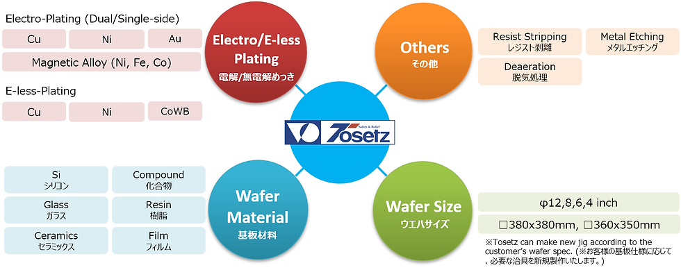
Tosetz offers a wide range of services, including electroplating of Cu, Au, Ni, magnetic alloy (Ni/Fe/Co) , and electroless plating, for wafers, resin, and ceramic substrates. We can also evaluate electroless plating of tungsten alloys with cobalt and nickel, which have a stronger copper diffusion barrier effect than conventional electroless Ni plating.
We also specialize in Invar (NiFe36) electroplating, which has low coefficient of thermal expansion and is expected to be used as a thermal stress buffer material.
Please see the article on Invar plating here.
In cooperation with wafer processing manufacturers, we can evaluate the effects of dissolved oxygen in chemical solutions and pure water in cleaning processes, as well as pre- and post-treatment in plating processes, resist stripping, wet etching, and other wet processes using deaeration systems to improve the quality of all wet processes.
This blog post here also contains details about the analysis and measurement environment, so please take a look if you are interested.
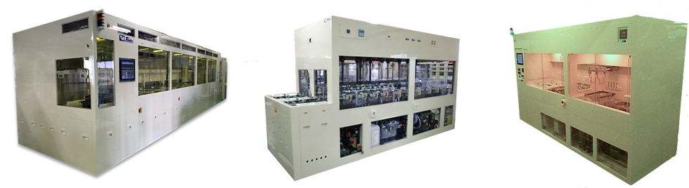
Tosetz proposals for prototype and mass production equipment
Tosetz designs and manufactures manual, semi-automatic, and automatic electroplating for Cu/Ni/Au continuously layered or electroless plating equipment that can deposit plating films with excellent thickness uniformity to meet customer needs.
We can customize the design of prototype and mass production equipment to meet your needs, from automatic transfer mechanisms that can handle thin and fragile wafers from small diameter to 12 inch and large square substrates.
We can also offer proposals that include resist stripping equipment and etching equipment.
Lastly
What do you think?
Tosetz will also help you with the development and mass production of your next-generation power semiconductors.
If you have any concerns about prototyping, contract processing, joint development, etc., please feel free to contact us below!
Click here if you are interested in Tosetz plating technology.
↓


Comments